Sunday, 9 June 2013

Tugas ELDA Ke-5

1. What are the parameters for controlling power is a transmission line?
Jawab:
Line impedance, magnitude and phase angle of bus voltage
2. What is the basic principle of shunt compensator?
Jawab:
rrr
Figure shows the principle and theoretical effects of shunt reactive power compensation in a basic ac system, which comprises a source V1, a transmission line and typical inductive load. Figure (a) shows the system without compensation, and its associated phasor diagram. In the phasor diagram the phase angel of the current has been related to the load side, which means that active current Iis in phase with the load voltage V2. Since the load is assumed inductive, it requires reactive power for proper operation, which must be supplied by the source, increasing the current flow from the generator and through the lines. If reactive Is supplied near the load, the line current is minimized, reducing power losses and improving voltage regulation at the load terminals. This can be done with a capacitor, with a voltage source, or with a current source. In figure (b), a current-source device is being used to compensate the reactive component of the load current (IQ). As a result, the system voltage regulation is improved and the reactive current component from the source is almost eliminated.
A current source or a voltage source can be used for reactive shunt compensation. The main advantages of using voltage or current source VAR generator (instead of inductor or capacitor) are that the reactive power generated is independent  of the voltage at the point of connection and can be adjusted in a wide range.
3. What is the TCR?
Jawab:
Thyristor-Controlled Reactor adalah jenis dari compensator yand dibuat dari sebuah supplai induktansi melalui ac -ac converter menggunakan dua buah thyristor anti paralel.
4. What is the TSC
Jawab:
Thyristor switched capacitor) adalah rangkaian yang digunakan untuk mengkompensasi daya reaktif pada sistem elektronika daya. TSC terdiri atas kapasitor daya yang disambung seri dengan bidirectional thyristor, dan biasa digunakan membatasi induktor (reaktor). TSC merupakan komponen yang penting bagi Static VAR Compensator (SVC).
5. What is the SVC
Jawab:
SVC adalah mengatur besarnya VAR dan tegangan dengan mengatur besar daya reaktif intduktif dari reaktor serta menyediakan daya reaktif dengan reaksi yang cepat
6. What is the statcom
Jawab:
Static Synchronous Compensator, injeksi arus melalui tranformator yang berfungsi sebagai penyedia Volt Ampere Reactive (VAR) untuk menjaga kestabilan voltase pada jaringan transimi yang panjang dan berbeban tinggi
7.  What is the basic principle of series compensation
Jawab:
Pada series compensation, the FACTS (Flexible AC transmission system) dihubungkan seri dengan sistem daya. Hal ini bekerja sebagai pengontrol tegangan sumber. Induktansi seri selalu digunakan pada semua jalur transmisi AC. Pada jalur yang panjang, ketika arus besar mengalir, hal ini menyebabkan drop tegangan yang besar. Untuk mengkompensasi tegangan drop ini, kapasitor seri dihubungkan untuk mengurangi efek dari induktansi.
8. What is the TSSC
Jawab:
Thyristor Switched Series Capacitor merupakan rangkaian seri kapasitor yang dihubung singkat oleh sebuah reaktor thyristor-switched.
9. What is the TCSC
Jawab:
Thyristor Controlled Series Capasitor yang berfungsi sebagai pengendali impedansi dari jaringan transimis
10. What is the FCSC
Jawab:
Forced Commutation Controlled Series Capacitor merupakan rangkaian yang dibentuk oleh kapasitor seri dengan kontroler. Cara kerja FCSC sama dengan TSC, kecuali pada switch  diganti dengan alat pendorong secara komutatif.
11. What is a series stacom
Jawab:
SSSC (static Synchronous series compensator) yang berarti rangkaian seri alat Flexible AC transmission system /FACTS menggunakan elektronika daya untuk mengontrol aliran daya dan meningkatkan osilasi daya menguasai jalur daya. The SSSC menginfus sebuah tegangan Vs dihubung seri dengan jalur transmisi yang tekoneksi.
12. What is the basic principle of phase angle compensation
Jawab:
Prinsip dasar kompensasi sudut phasa adalah untuk meningkatkan strategi LVRT (Low voltage ride through) yang ada.
13. What is the phase shifter
Jawab:
Penghubung dua sistem dengan phasa yang berlebihan atau perbedaan phasa yang tidak terkontrol. namun hal ini megizinkan pengaturan besar beda phasa.
14. What is quadrature booster (QB)
Jawab:
Quadrature booster dapat menyediakan tegangan dengan instalasi yang sesuai dengan koneksi pada trafo. Trafo menyediakan pergeseran phasa yang penting atau tegangan quadrature sekitar sistem untuk mengendalikan arus yang sesuai.
15. What is the UPFC
Jawab:
Unified Power Flow Controller, dapat mengendalikan impedansi transimis, tegangan dan sudut fasa. UPFC merupakan kombinasi statcom dan SSSC.
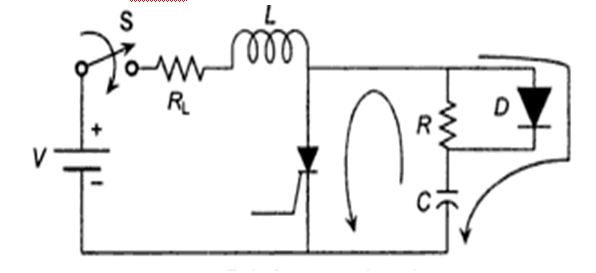
16. What are the rule for transient free switching of thyristor
jawab:
  • To turn a thyristor (or triac) ON, a gate current  ≥ IGT must be applied until the load current is ≥ IL. This condition must be met at the lowest expected operating temperature.
  • To turn off (commutate) a thyristor (or triac), the load current must be < IH for sufficient time to allow a return to the blocking state. This condition must be met at the highest expected operating temperature.
  • When designing a triac triggering circuit, avoid triggering in the 3+ quadrant (MT2-, G+) where possible.
  • To minimise noise pickup, keep gate connection length to a minimum. Take the return directly to MT1 (or cathode). If hard wired, use twisted pair or shielded cable. Fit a resistor of 1kΩ or less between gate and MT1. Fit a bypass capacitor in conjunction with a series resistor to the gate. Alternatively, use an insensitive series H triac.
17. What are switch capasitor
jawab:
18. What is the SSVC
Jawab:
Solid State Var Compensator bekerja pada tegangan inverter PWM. Inverter dihubungkan oleh tegangan AC melalui reaktor. Sebuah kapasitor DC terhubung ke sisi DC dari VAR compensator. Kapasitor berfungsi mempertahankan rippe tegangan DC pada input serta menyimpan daya reaktif, lalu SSVC terhubung ke beban melalui LPF orde dua yang mengurangi arus harmonik komponen sebagai jaringan utilities.

Tugas ELDA ke-4

1. What is a heat sink?
heat sink is a passive heat exchanger component that cools a device by dissipating heat into the surrounding air
2. What are the precautions to  be taken in mounting a device on a heat sink?
The device must be mounted properly on the heat sink to obtain the correct mounting pressure between the mating surface.
3. What is a heat pipe?
A heat pipe or heat pin is a heat-transfer device that combines the principles of both thermal conductivity and phase transition to efficiently manage the transfer of heat between two solid interfaces
4. What are the advantages and disadvantages of heat pipe?
Advantages:
The device may be cooled by heat pipes partially filled with low-vapor-pressure liquid.
Disadvantages:
Heat pipes must be tuned to particular cooling conditions. The choice of pipe material, size and coolant all have an effect on the optimal temperatures in which heat pipes work.
5. What are the advantages and disadvantages of water cooling?
Advantages:
Water is inexpensive and non-toxic. The advantages of using water cooling over air cooling include water’s higher specific heat capacity, density, andthermal conductivity. This allows water to transmit heat over greater distances with much less volumetric flow and reduced temperature difference.
Disadvantages:
Water accelerates corrosion of metal parts and is a favorable medium for biological growth. Dissolved minerals in natural water supplies are concentrated by evaporation to leave deposits called scale. Cooling water often requires addition of chemicals to minimize corrosion and insulating deposits of scale and biofouling.
6. What are the advantages and disadvantages of oil cooling?
Advantages:
  • Oil has a higher boiling point than water, so it can be used to cool items at a temperature of 100°C or higher. However, pressurised water-cooling may also exceed 100°C.
  • Oil is an electrical insulator, thus it can be used inside of or in direct contact with electrical components.
  • Oil is already used as a lubricant, therefore it may serve in a double use arrangement.
Disadvantages:
  • Coolant oil may be limited to cooling objects under approximately 200°C – 300°C.
  • Parts are hard to take out and put in after the oil is put in.
  • Water is almost universally available in case coolant needs to be added to the system, but oil is not.
  • Unlike water, oil may be flammable.
7. What is it necessary to determine the instantaneous junction temperature of a device?
The instantaneous junction temperature must always be maintained lower than the acceptable value.
8. What is polarized snubber?
f
The changing is quick and through the diode when the thyristor is switched on, the  capacitor discharges through R.
 9. What is nonpolarized snubber?
snubber is classed as polarized or non-polarized depending on whether energy moves in or out of the snubber on one edge of the switching waveform
 10. What is the typical value of damping factor for RC snubber?
 The damping factor is proportional to the ratio of the circuit loss and its surge impedance. It determines the trade off between dv/dt and peak voltage. Damping factors between 0.01 and 1.0 are recommended
 11. What is considerations for the design of optimum RC-snubber components?
  • Voltage rating of snubber capacitor and snubber resistor
When selecting the capacitor, a number of different voltage ratings has to considered. The main parameters are the rms and the repetitive voltage ratings. The rms voltage the capacitor sees is dependent on the application and on the way it is used. For a 6-pulse bridge, the rms voltage will be a function of the firing angle. It reaches its maximum for firing angles of 0° or 180 °at 0.90 times the sinusoidal rms voltage at the 3-phase input of the bridge. Some capacitor suppliers do not rate their capacitors with an rms current but either with a “rated” AC voltage, which is then defined as either the maximum repetitive peak voltage in operation or as the maximum repetitive peak-to-peak voltage. Peak voltages for this consideration do not include the relatively short transient switching overvoltages discussed above.
  •  Power rating of snubber Resistor
When the overvoltage calculation is done as discussed above, the resistance value for the snubber resistor is calculated and it is fairly simple to calculate the energy dissipated in the resistor during thyristor turn-off as well. This information is though not enough to define the appropriate resistor.
 12. What are the characteristics of selenium diodes?
Selenium diodes work much like any other diode. They allow current to flow in a forward direction and block current from flowing in the opposite direction. They have a higher forward bias voltage then silicon and as such generate much more heat then a comparable silicon diode. Most selenium diodes will therefore have an integrated heat sink that helps to dissipate all the heat generated.
 13. What are the advantages and disadvantages of selenium voltages suppressers?
Advantages:
All things being equal, a full wave rectifier will result in a slightly higher DC voltage with less ripple
Disadvantages:
The gradual drop in voltage can destroy a set of outputs before you even know there’s a problem
 14. What are the characteristics of varistor?
The relationship between voltage and current of a varistor can be approximated to: V = C x Iβ
where:
V = voltage
C = varistor voltage at 1 A
I = actual working current
β = tangent of angle curve deviating from the horizontal
 15. What are the advantages and disadvantages of selenium voltages varistor?
Advantages:
Used for protection against transient over voltages
Disadvantages:
Low forward voltage
 16. What is an arcing time of a fuse?
The amount of time that passes from the instant the fuse element or link has melted until the overcurrent is interrupted or cleared.
 17. What is a clearing time of a fuse?
This is the total opening time of a fuse from the occurrence of an overcurrent until the fuse stops current flow. This is the sum of link melting and arcing time.

Tugas ELDA ke-3

1. What is BJT?
Jawab:
BJT (Bipolar Junction Transistor) adalah salah satu dari dua jenis transistor. Cara kerja BJT daoat dibayangkan sebagai dua dioda yang terminal positif atau negatifnya berdempet, sehingga ada tiga terminal. Ketiga terminal tersebut adalah emiter (E), kolektor (C) dan basis (B).
2. What is the type of BJT ?
Jawab:
Tipe pertama terdiri dari dua daerah n yang dipisahkan oleh daerah p (npn), dan tipe lainnya terdiri dari dua daerah p yang dipisahkan oleh daerah n (pnp). Sambungan pn yang menghubungkan daerah base dan emitter dikenal sebagai sambungan base-emiter (base-emitter junction), sedangkan sambungan pn yang menghubungkan daerah base dan kolektor dikenal sebagai sambungan base-kolektor (base-collector junction).
3. What is the differences between npn and pnp transistor ?
Jawab:
  • NPN
Prinsip kerja dari transistor NPN adalah: arus akan mengalir dari kolektor ke emitor jika basisnya dihubungkan ke ground (negatif). Arus yang mengalir dari basis harus lebih kecil daripada arus yang mengalir dari kolektor ke emitor, oleh sebab itu maka ada baiknya jika pada pin basis dipasang sebuah resistor.
  • PNP
Prinsip kerja dari transistor PNP adalah arus akan mengalir dari emitter menuju ke kolektor jika pada pin basis dihubungkan ke sumber tegangan (diberi logika 1). Arus yang mengalir ke basis harus lebih kecil daripada arus yang mengalir dari emitor ke kolektor, oleh sebab itu maka ada baiknya jika pada pin basis dipasang sebuah resistor.
5. What are the three regions of operation for  BJT?
Jawab:
  •  Cut-off
Transistor menjadi kondisi off, IC=0. Daerah dimana VCE masih cukup kecil sehingga arus IC=o atau IB=0.
  • Active
Transistor beroperasi sebagai penguat dan IC=β x IB. Daerah kerja transistor yang normal adalah pada daerah aktif, yaitu ketika arus ICkonstan terhadap berapapun nilai VCE. IC sangat bergantung pada besar arus IB. Daerah kerja ini biasa disebut daerah liniear.
  • Saturation
Transistor menjadi kondisi on, IC=ISAT. Daerah saturasi mulai dari VCE=0-0,7volt (transistor silikon). Ini diakibatkan oleh efek p-n junction kolektor-basis yang membutuhkan tegangan yang cukup agar mampu mengalirkan elektron sama seperti dioda.
6. What is the β of BJT
Jawab:
β= Iβ/Ic
Beta (β) didefinisikan sebagai besar perbandingan antara arus kolektor dengan arus basis. Yang artinya β adalah parameter yang menunjukan kemampuan penguatan arus (current gain) dari suatu transistor.
7. What is the differences between β and β force
Jawab:
beta (β) didefinisikan sebagai besar perbandingan antara arus kolektor dengan arus basis. β force  ini terjadi saat saturasi karena arus kolektor hampir tetap konstan. Sehingga beta forced merupakan perbandingan arus kolektor dengan arus basis.
8. What is transconductance of BJT
Jawab:
transconductance, gm, didefinisikan sebagai perubahan arus kolektor dibagi dengan perubahan tegangan basis-emitor.
9. What is ODF
Jawab:
ODF(overdrive factor). Faktor overdrive adalah perbandingan dari arus basis dengan arus di ujung saturasi.
10.What is MOSFET
Jawab:
MOSFET (Metal-oxide semiconductor FET) merupakan transistor yang memiliki kaki drain, source dan gate. Namun pada kaki gate terisolasi suatu bahan oksida yang terbuat dari bahan metal aluminium.
11. What is the types of MOSFET
Jawab:
Depletion mode & enhancement mode
ff
12. What is the switching model of and chanel MOSFET?
Jawab:
Pada umumnya transistor mosfet digunakan sebagai saklar. Pada mosfet enhancement-mode atau biasa disebut e-mosfet. Parameter yang penting pada transistor e-mosfet adalah resistansi drain source. Biasanya yang tercantum pada data sheet ialah resistansi saat transistor ON. Resistansi itu yang disebut dengan RDS(ON). Untuk aplikasi power switching, semakin kecil RDS(ON) maka semakin baik transistor tsb. Karena akan memperkecil rugi-rugi disipasi daya dalam bentuk panas dan parameter arus drain ID(MAX) dan disipasi daya maksimum PD(MAX). Pada transistor mosfet depletion mode dapat bekerja on mulai dari VGS negatif sampai positif
 Mosfet dapat berfungsi sebagai saklar, dengan ketentuan saklar akan on ketika
VGS≥VTH dan VDD≥VTH.
VTH merupakan V treshold dimana mosfet mulai bekerja.
14. What is IGBT ?
Jawab:
IGBT (insulated gate bipolar transistor)  adalah semikonduktor yang setara dengan gabungan sebuah BJT dan sebuah MOSFET. Berfungsi sebagai komponen saklar untuk aplikasi daya.
15. What is the purpose the shunt and series snubber in transistor ?
Jawab:
a. Snubber pada transistor
  • Semakin besar ukuran kapasitor pada snubber, kerugian daya pada suatu transistor akan semakin kecil namun akan semakin besar daya serap oleh resistor pada snubber.
  • Mengurangi total kerugian switching dan kerugian pada transistor
  • Mengurangi nilai tegangan dan arus yang tinggi pada transistor
b. Shunt pada transistor

Tugas ELDA ke-2

1. Sebutkan macam-macam dioda daya
Jawab:
General Purpose Diode
-       High reverse recovery time, typically 25 us,
-       Use for low speed application
-       Low frequency up to 1 KHz
-       Rating current from less than 1 A
-       Voltage rating from 5 V to 50 KV
Fast Recovery Diode
-       Low recovery time less then 5 us
-       Use for chopper and inverter
-       Rating current from less than 1 A
-       Voltage rating from 5 V to 3 KV
Schottky Diode
-       Low forward voltage drop
-       Use for high current low voltage rectifier
-       Rating current from  1 A – 300 A
-       Voltage rating  to  100V
2. Gambarkan dan jelaskan symbol dan karakterisitik dioda!
Jawab:
Dioda merupakan komponen elektronika yang mempunyai dua elektroda (terminal), dapat berfungsi sebagai penyearah arus listrik. Ada dua jenis dioda yaitu dioda tabung dan dioda semikonduktor. Dengan kata lain sambungan semikonduktor P-N hanya dapat mengalirkan arus ke satu arah. Dioda semikonduktor dibuat dari sambungan P-N ini. Terminal pada P disebut anoda, sedang terminal N disebut katoda. Gambar a menunjukkan sambungan P-N nya, sedang gambar b menunjukkan lambang atau simbolnya. Arah panah menunjukkan arah hole (arus listrik) jika diberi tegangan maju (prasikap maju).Saat ini diode yang paling umum dibuat dari bahan semikonduktor seperti silikon atau germanium.
a
Karakteristik dioda dapat ditunjukkan oleh hubungan antara arus yang lewat dengan beda potensian ujung-ujungnya. Karakteristik dioda pada umumnya diberikan oleh pabrik, tetapi dapat juga diselidiki sendiri. Diode sebenarnya tidak menunjukkan karakteristik kesearahan yang sempurna, melainkan mempunyai karakteristik hubungan arus dan tegangan kompleks yang tidak linier dan seringkali tergantung pada teknologi atau material yang digunakan serta parameter penggunaan.
3. Apa yang dimaksud dengan arus bocor ( leakage current ) pada dioda?
Jawab:
Adalah sebuah nilai maksimum dari reverse current pada teperetur maksimum junction dan maksimum repetitive peak reverse voltage.
 4. Apa yang dimaksud dengan reverse recovery time pada dioda?
Jawab:
Dapat didefinikan sebagai waktu interval antara arus instan yang melewati nol selama beralih dari condisi forward ke kondisi reverse blocking.
 5. Apa yang dimaksud dengan reverse recovery current pada dioda?
Jawab:
Arus maju akan diturunkan menjadi nol (karena perilaku natural rangkain dioda atau dengan menerapkan tegangan mundur), dioda meneruskan konduksi karena pembawa minoritas yang tersisa dalam sambungan pn dan material semikonduktornya. Pembawa minoritas memerlukan waktu yang cukup untuk menyusun ulang dengan pengisian lawannya dan untuk dinetralkan. Waktu ini disebutkan reverse recovery time (waktu pemulihan yang balik).
 6. Apa yang dimaksud dengan faktor kelunakan?
Jawab:
Softness factor adalah paramater tdan tb. Paramater tadalah interval antara zero crossing pada arus dioda dan ketika itu berubah menjadi IRR. Parameter twaktu  interval dari maksimum arus reverse recovery ke 0.25 dari IRR.
 7. Sebutkan jenis-jenis pemlihan diode!
Jawab:
a. Soft recovery
b. Absurb recovery
 8. Apa yang menyebabkan reverse recovery time pada diode?
Jawab:
Carrier minority yang membutuhkan waktu tertentu un menkombinasi ulang dengan pengisian berlawanan dan kembali dinaturalisasi.
 9. Apa yang diperlukan untuk menggunakan fast recovery dioda untk high speed switching?
Jawab:
a. Rating arus dari kurang dari 1 Ampere sampai ratusan Ampere.
b. Rating tegangan 50 V samapai sekitar 3 kV
 10. Apa yang dimaksud dengan forward recovery?
Jawab:
Ketika diode pada reverse-bias, sebuah arus bocor mengalir pada minority carrier. Kemudian aplikasi dari forward voltage akan melawan dioda untuk membawa arus pada arah maju.
 11. Apa perbedaan utama antara pn junction diode dengan schottky diode?
Jawab:
Permasalahan charge storage pada pn juction dapat dieliminasi (diminimalisasi)
 12. Apa keterbatasan dari dioda schottky?
Jawab:
Tegangan maksimum yang diperbolehkan terbatas pada 100 V. Rating arus antara 1 dan 300 A.
13. Apa ciri dari recovery time pada general purpose diode?
Jawab:
a. High reverse recovery time
b. Low speed application
c. Current rating less than 1 A to several hundreds Ampere
d. Voltage rating from 50 V to 5 kV
 14. Apa ciri dari recovery time pada fast recovery diode?
Jawab:
a. Low recovery time, normali less than 5 us
b. Current rating 1 A to hundreds of ampere
c. Voltage rating 50 V to 3 kV
 15. Apa ciri dari maximum juction temerature dari dioda?
Jawab:
Dapat menahan tanpa kegagalan akibat hilang termal
 16. Apa tujuan dari current-limiting inductor?
Jawab:
Untuk mencegah kerusakan dioda yang diakibatkan kenaikan forward current yang sangat besar, cenderung tak terhingga. Hal ini mengakibatkan puncak arus reverse current dioda menjadi sangat besar, maka di tambahkan induktor agar batas waktu aktif dioda tetap rendah.
 17. Apa permasalahan pada series-connected diode dan apa solusinya?
Jawab:
Dioda tidak dapat menemukan tegangan yang dibutuhkan dan dioda yang terkoneksi secara seri meningkatkan kemampuan reverse blocking
Solusi: dengan memaksa nilai tegangan menjadi sama dengan menghubangakan dengan resistor secara silang pada tiap dioda.
 18. Apa permasalahan pada parallel-connected diode dan apa solusinya?
Jawab:
Pada aplikasi daya tinggi, dioda yang terhubung secara paralel dapat meningkatkan capasitas current-carrying untuk mencapai syarat arus yang diinginkan. Pembagian arus pada dioda akan mengikuti respective forward voltage drops.
Solusi: dengan memilih dioda dengan forward voltage drop yang sama atau dioda yang satu tipe.
 19. If two diodes are connected in series with equal-voltage sharing, why do the diode leakage current?
Jawab:
Jika dioda dihubung seri dengan tegangan bagi sama maka akan menjadikan arus bocor pada setiap dioda akan berbeda karena karena perbedaan tegangan pembatas yang besar.
b
Untuk mengatasi kebocoran arus, dipasang resistor secara pararel sehingga tegangan pada setiap dioda menjadi sama.
c
12-1 The reverse recovery time of a diode is trr = 5 µs and the rate of fall of the diode current is di/dt = 80 A/µs. If the softness factor (SF) = 0,5. Determine the :
a. Storage charge, QRR
b. Peak reverse current, IRR
Answer :
d
12-2 The peak input voltage of a single phase half-wave diode rectifier is  Vm = 169 V at 60Hz and load resistance is RL =1.2 Ω. The reverse recovery time is trr= 4 µs. If the softness factor SF= 0, Determine the :
a. Storage charge, QRR
b. Peak reverse current, IRR
Answer :
e
12-3 Four IR 300 A, 800 V diodes of type R23AF are used for the single-phase bridge rectifier as shown in the figure. The   rms value of the input voltage is Vs = 220 V at 1.5 kHz and the load resistance is R = 0,47 Ω. The junction temperature and ambient temperature are TJ = 15oC and TA= 25oC, respectively. Determine: (a) Average power loss,PD; (b) Instantaneous forward voltage drop,vF; (c) Recovery charge, QRR; (d) Reverse recovery time,trr; (e) Case temperature, TC; (f) Thermal resistance of  heat sink, RthSA. Assume double-sided cooling and the case-to-sink thermal resistance of RthCS = 0,03oC/W
Answer:
Vs = 220 V; fs = 1,5kHz; R = 0.47 Ω
TJ = 15 oC; TA = 20 oC
  1. PD
Vm =  = 311,127 Volt
Tegangan output raa-rata : Vdc = 0,6366. Vm = 0,6366. 311,127 = 198,06 V
Arus beban rata-rata : Idc = 198,06/ 0,47 = 421,40 A
Rata-rata arus forwarddioda : IF(AV) = 421,4/2 =210,7 A
Dari kurva karakteristik Power Loss; Untuk 180o, maka diperoleh besarnya daya yang hilang PD @ 250 W
  1. vF
dari kurva forward characteristics diperoleh tegangan threshold V(TO) = 0.6V
r@  = 2,5 mΩ
sehingga diperoleh i = (311,127/0,47) sin wt
vF = 0,6 + 2,5 x 10⁻³ x
=
  1. QRR
IFM =
Untuk IFM = 661,127 A dan di/dt = 6,2  maka dengan menggunakan metode interpolasi diperoleh QRR = 14
  1. tRR
SF = tb/ta = 0,8; trr = ta + tb = 1,8ta
trr =  = 285 µs
  1. TC
dari datasheet dioda diketahui, RthJC = 0,09oC/W
Tc = TJ – RthJC.PD
= 125 – 0,09 x 250
= 102,5 oC
  1. RthSA
PD(RthJC + RthCS + RthSA) = TJ – TA
PD(RthJC + RthCS + RthSA) = 125 – 25
PD(RthJC + RthCS + RthSA) = 100
RthSA = 0,28oC/W